SMTStencil
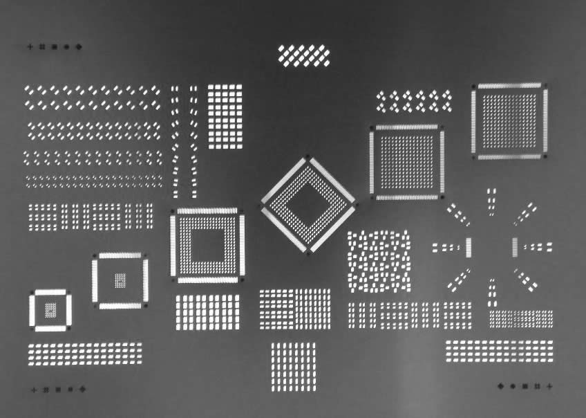
Electroformed SMT Stencils
Why electroformed Stencils?
Precision Tech uses the latest technology Electroformed Stencils: SMT Stencils.
Features & Benefits:
- The smooth trapezoidal sidewalls of an electroformed stencil allows for better paste release compared to polished laser or etched stencils. Electroform stencils provide fine and ultra-fine pitch apertures with paste transfer efficiencies at 95% and above, while minimizing bridging.
- Since the process occurs at an atomic scale, the aperture tolerances are in the micron range. Typically, +/- 10 microns (.0004″) are achieved.
- Electroform foils are harder than full hard stainless steel of comparable thickness, providing for longer stencil life (hardness 500 Hv and greater). This durability is advantageous for high-volume runs.
- Nickel has a lower coefficient of friction compared to stainless steel, which allows for a better roll of the solder paste and decreases wear on squeegee blades.
- Allows for thinner stencils due to the increase in paste transfer efficiencies.
- Can mean an increase in production yields due to lower numbers of re-works.
- Stencils and foils can be produced in a non-standard thickness, if required, as well as step up, step down, and recessed areas (i.e. 2.4, 4.2, 5.7 etc)
- Large aperture counts can be completed faster and more efficiently with an electroform stencil due to the electroform process itself. This allows for a denser image area without any distortion due to heat transfer caused by laser cutting. (pad count: 1 to unlimited)

Step Stencils
Precision Technologies has the technical ability to manufacture step stencils in both single process and dual process. Today’s complex PCBs with the various components require different solder paste volumes. Precision Tech has the technical expertise to optimize the stencil by using various foil thicknesses on the same stencil, this allows the ability to control solder paste deposit in fine pitch areas while printing sufficient solder on coarse pitch areas.
Single Process
Our single process uses Photo Chemical matching (PCM), this allows different areas to be etched to lower the thickness of the foil, which in turn decreases the paste deposit in these same areas.

Dual Process
Our dual process follows the Step Stencil Process (image above), which can be engineered by a combination of PCM and laser cutting. First, the foil is chemically etched in the areas requiring less paste (for fine pitch components). Then the foil is placed into the laser machine to cut the apertures, offering greater accuracy and more precise apertures.
Please call our sales team at 1-888-228-9440 for a quote or to learn more information on our SMT stencils!
get started now
888-228-9440
For a Quick-Turn on Affordable PCB Fabrication & Assembly


